Unity Semiconductor (UnitySC), the France-based semiconductor inspection solution provider, announced that it has demonstrate the capability of detecting topographic defects on GaAs wafers for VCSEL in LiDAR and 3D recognition applications.
On top of common Surface Scanning Inspection Systems (SSIS) and Automatic Optical Inspection (AOI) systems, UnitySC noted that it is able to find out defects that are not visible on standard optical inspection systems. These defects do not scatter or absorb light, and can only be revealed by their topography but they can lead to device failure later on the process. For example, during the production of the Bragg grating reflectors, these topographic defects can lead to wrong Bragg period or, in some specific cases, to stress-induced cracks. These failures can happen during the process or after system delivery under heat or stress conditions resulting in system failure.
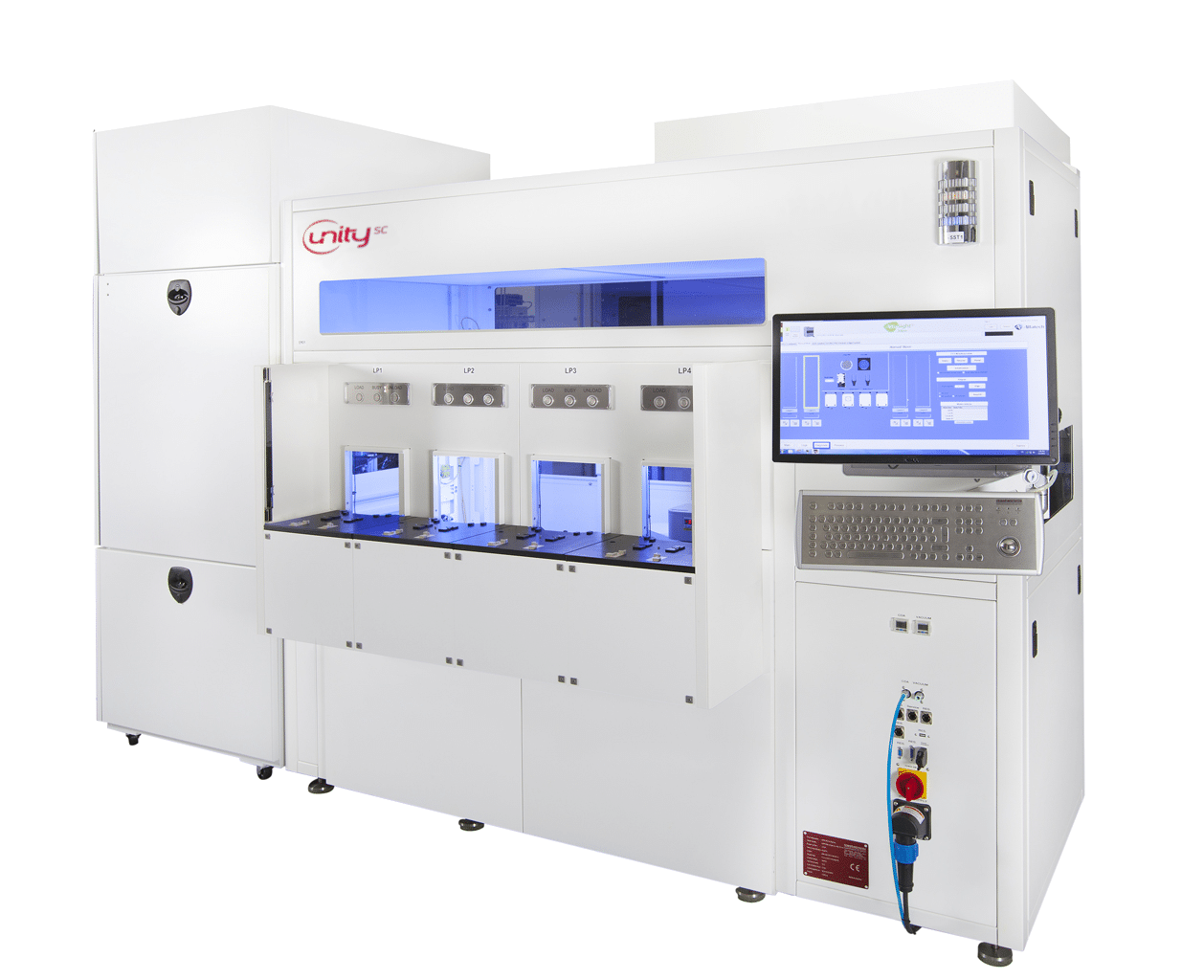
Thanks to the Phase Shift Deflectometry technology (PSD) embedded inside the LIGHTsEE™ series, these defects can be easily detected. The PSD provides a full wafer, non-contact, high throughput solution with a height sensitivity below 5nm. Since the acquisition is made without moving the substrate, it is stress-free and compliant with any fragile substrate.

(Image: UnitySC, LIGHTsEE™ series)
This technology was demonstrated with a major VCSEL manufacturer and revealed a yield improvement and a decrease in device failures by systematically suppress dies impacted by such defects. Therefore, by using the PSD in incoming quality control, VCSEL manufacturers can further increase their yield and improve their supply chain.
