According to LEDinside’s 2019 Micro LED Next Generation Display Key Technology Report, Micro LED possesses excellent features no matter in high brightness, high contrast, high response time and power saving, which are all better than LCD and OLED. With Micro LED, various applications, such as watch, mobile phone, automotive display, AR, VR, monitor, TV and large display will develop towards a higher level in the future. According to LEDinside, although Micro LED technology faces many challenges, compared with two years ago, the current technological progress has been much improved. The early patented technology has already appeared in the physical sample display machine. In the future, Micro LED’s commercialization will be driven by the growth of Micro LED technology. In addition, the manufacturing process of Micro LED is complex and the requirement becomes stricter. The raw materials, process consumables, production equipment, testing instruments and auxiliary fixtures used in the process require sophisticated specifications and relatively high precision.
Micro LED technology bottleneck analysis
At present, there are nine bottlenecks, including epitaxy, chip, mass transfer, full color, bonding, power drive, backplane, inspection and repairing technologies. This research report will conduct in-depth discussion and analysis on the bottleneck of Micro LED technology.
Epitaxy Technology: At present, one of the challenges of Micro LED epitaxy technology is to improve wavelength uniformity and thickness uniformity. Thus, the wavelength will be more concentrated and the back-end inspection cost of epitaxy manufacturers can be greatly lowered. Besides, when LED chip is reduced to less than 100µm, the problem of unevenness caused by cutting damage around the LED chip may lead to electricity leakage and affect the overall luminous characteristics.
Chip Manufacturing Process Technology: Because of mass transfer manufacturing process, chips need to go through structural weakening in order to be picked up from the temporary substrate. In order to avoid the damage of chips during mass transfer manufacturing process, ALD process is required to protect and insulate the chips.
Mass Transfer Technology: Stamp pick & place technology can be applied to products greater than 10µm, but there may be problems for UPH and transfer equipment’s precision and stability. Fluidic assembly technology can be applied to products greater than 20µm. Although UPH can be increased, three transfer times are required to achieve full color. Laser transfer technology can be applied to products greater than 1µm, but the cost of laser equipment is high and will be a burden of initial investment.
Full Color Technical Solution: RGB chip color conversion solution confronts with problems like insufficient luminance efficacy and low yield in regard to technology of less than 20µm. Instead, quantum dot technology can fill this gap. However, some problems facing quantum dot solutions like coating evenness and reliability remain to be broken through.
Bonding Technology: Because Micro LED chip is too small, the large metal content of the solder paste can easily cause the p-pad and n-pad conduction of Micro LED to form a micro short circuit. Therefore, the adhesion technology will be a key challenge for Micro LED process. Currently, there are four directions: Metal Bump, Adhesive, Wafer Bonding and Micro Tube.
Driver Technology: In the active matrix drive array, each pixel is connected to the circuit and driven separately, which will allow Micro LED to operate at a lower current while maintaining brightness throughout the entire illumination time without significant loss of display brightness, but Micro LED drive current is extremely small, which makes the circuit design complicated and the space layout of drive power module will be denser.
Backplane Technology: There are four types: glass, flexible substrate, silicon substrate and PCB. At present, PCB backplane is the most widely used, mainly because of its high compatibility. The splicing can be used to meet various required sizes, and the corresponding substrate can be selected according to the requirements to be the corresponding backplane.
Inspection & Testing Technology: Micro LED application products use a large number of chips. Besides, the Photoluminescence and Electroluminescence of Micro LED module have to be detected correctly and rapidly. It is necessary to adopt mass testing method to reduce time and cost. Identifying good product quickly and accurately is a major problem in the manufacturing process and one of the main reasons for the bottleneck of current Micro LED testing technology.
Repairing Technology: In terms of Micro LED repairing solution, currently there are ultraviolet irradiation repairing technology, laser welding repairing technology, selective pick repairing technology, selective laser repairing technology and redundancy circuit design solution.
In January 2019, LEDinside has analyzed the key technologies of 2019 Micro LED next generation display. For more information, please call or email us. Thank you!
LEDinside 2019 Micro LED Next Generation Display Key Technology Report
Release Date: January 31, 2019
Format: PDF
Language: Traditional Chinese / English
Pages: 219
Quarterly Update: Micro / Mini LED Market Perspective Analysis - Vendor Dynamics, New Technology Import, Display Week / Touch Taiwan Direct Strike (March, June, September 2019; Approx. 10-15 pages/quarter)
Chapter 1 Definition and Market Scale of Micro LED
Product Definition of Micro LED
Analysis and Prediction of Micro LED Market Value
Analysis and Prediction of Micro LED Output Volume
Estimation of Micro LED Display Penetration Rate
Chapter 2 Micro LED Applications and Technology Development
Micro LED Product Overview
Micro LED Product Specifications Overview
Micro LED Applications- Specifications of Head Mounted Device
Micro LED Applications- Cost of Head Mounted Device
Micro LED Applications- Shipment Volume of Head Mounted Device
Micro LED Applications- Specifications of Wearable Device
Micro LED Applications- Cost of Wearable Device
Micro LED Applications- Shipment Volume of Wearable Device
Micro LED Applications- Specifications of Handheld Device
Micro LED Application- Cost of Handheld Device
Micro LED Application- Shipment Volume of Handheld Device
Micro LED Application- Specifications of IT Device
Micro LED Application- Cost of IT Display
Micro LED Application- Shipment Volume of IT Device
Micro LED Application- Specification of Automotive Display
Micro LED Application- Cost of Automotive Display
Micro LED Application- Shipment Volume of Automotive Display
Micro LED Application- Specifications of TV
Micro LED Application- Cost of TV
Micro LED Application- Shipment Volume of TV
Micro LED Application- Specifications of LED Display
Micro LED Application- Cost of LED Display
Micro LED Application- Shipment Volume of LED Display
Chapter3 Micro LED Patent Analysis
2000-2018 Micro LED Patent Layout- Patent Family Analysis
2000-2018 Micro LED Patent Layout- Region Analysis
2000-2018 Micro LED Patent Layout- Technology Analysis
2000-2018 Micro LED Patent Layout- Manufacturer Analysis
2001-2018 Micro LED Patent Layout- Mass Transfer Technology Patent Family Analysis
Mass Transfer Technology- Patent Technology Overview
Mass Transfer Technology- Patent Technology Classification
2001-2018 Micro LED Patent Layout- Mass Transfer Technology Patent Family Analysis
Mass Transfer Technology- Brand Manufacturer Technology Layout Analysis
Mass Transfer Technology- Start-up and Research Institution Technology Layout Analysis
Chapter 4 Micro LED Technology Bottleneck and Solution
Micro LED Industry Technology Overview Analysis
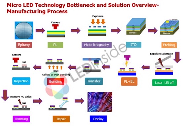
Micro LED Technology Bottleneck and Solution Overview- Manufacturing Process
Micro LED Technology Bottleneck and Solution Overview- LED Epitaxy and Chip Manufacturing Process
Micro LED Technology Bottleneck and Solution Overview- Transfer Technology/Bonding Technology/Drive and Backplane Technology
Chapter 5 Epitaxy Technology Bottleneck and Challenge Analysis
Epitaxy Technology- Solution
Epitaxy Technology- Epitaxial Wafer Structure and Light Emitting Principle
Epitaxy Technology- Epitaxy Emissive Layer Material and Luminous Efficacy
Epitaxy Technology- The Leakage Problem of Chip Miniaturization Causes the Drop of Luminous Efficacy
Epitaxy Technology- Equipment Technology Classification
Epitaxy Technology- Equipment Technology Comparison
Epitaxy Technology- Epitaxial Wafer Key Technology Classification
Epitaxy Technology- Epitaxial Wafer Key Technology Classification- Wavelength Uniformity
Epitaxy Technology- Epitaxial Wafer Key Technology Classification- Defect Control
Epitaxy Technology- Epitaxial Wafer Key Technology Classification- Increase of Utilization of Epitaxial Wafer
Epitaxy Technology- Applicability Analysis
Chapter 6 Chip Manufacturing Process Technology Bottleneck and Challenge Analysis
Chip Manufacturing Process Technology- Development of LED Chip Miniaturization
Chip Manufacturing Process Technology- LED Chip Production Process
Chip Manufacturing Process Technology- Structural Differences between Lateral Chip, Flip Chip and Vertical Chip
Chip Manufacturing Process Technology- Miniaturized LED Chip (Including Sapphire Substrate) Scribing Technology
Chip Manufacturing Process Technology- Miniaturized LED Chip (Excluding Sapphire Substrate) Scribing Technology
Chip Manufacturing Process Technology- Laser Ablation
Chip Manufacturing Process Technology- Structural Weakening and Insulating Layer
Chip Manufacturing Process Technology- Design of Structural Weakening
Chip Manufacturing Process Technology- Design of Transfer Head
Chip Manufacturing Process Technology- Differences between Traditional LED and Micro LED Chip Manufacturing Processes
Chapter 7 Mass Transfer Technology Bottleneck and Challenge Analysis
Mass Transfer Technology- Transfer Technology Classification
Mass Transfer Technology- Thin Film Transfer Technology Classification
Mass Transfer Technology- Thin Film Transfer Technology- Pick & Place Technology
Mass Transfer Technology- Thin Film Transfer Technology- Non-selective Pick Technology
Mass Transfer Technology- Thin Film Transfer Technology- Selective Pick Technology will Increase Wafer Utilization
Mass Transfer Technology- Thin Film Transfer Technology- Selective Pick Technology in Repair Application
Mass Transfer Technology- Thin Film Transfer Technology- Factors that Affect UPH
Mass Transfer Technology- Thin Film Transfer Technology- Solution of Increasing UPH for Large Transfer Head
Mass Transfer Technology- Thin Film Transfer Technology- Higher Transfer Head Accuracy Requirement
Mass Transfer Technology- Thin Film Transfer Technology- Comparison between Transfer Times and Wafer Utilization
Mass Transfer Technology- Thin Film Transfer Technology- Comparison between Cycle Time and UPH
Mass Transfer Technology- Thin Film Transfer Technology: Apple (LuxVue)
Electrostatic Adsorption + Phase Change Transfer
Mass Transfer Technology- Thin Film Transfer Technology: Samsung
Chip Transfer and Flip
Mass Transfer Technology- Thin Film Transfer Technology- Van der Waals Force Introduction
Mass Transfer Technology- Thin Film Transfer Technology: X-Celeprint
Van der Waals Force
Mass Transfer Technology- Thin Film Transfer Technology: ITRI
Electromagnetic Adsorption
Mass Transfer Technology- Thin Film Transfer Technology: Mikro Mesa
Adhesion and Reaction Force
Mass Transfer Technology- Thin Film Transfer Technology: AUO
Electrostatic Adsorption and Reaction Force
Mass Transfer Technology- Thin Film Transfer Technology: VueReal
Solid Printing
Mass Transfer Technology- Thin Film Transfer Technology: Rohinni
Alignment Pin
Mass Transfer Technology- Thin Film Transfer Technology- Fluidic Assembly Technology
Mass Transfer Technology- Thin Film Transfer Technology: eLux
Fluidic Assembly
Mass Transfer Technology- Thin Film Transfer Technology: PlayNitride
Fluidic Transfer
Mass Transfer Technology- Thin Film Transfer Technology- Laser Transfer
Mass Transfer Technology- Thin Film Transfer Technology- Laser Transfer Classification
Mass Transfer Technology- Thin Film Transfer Technology: Sony
Laser Transfer
Mass Transfer Technology- Thin Film Transfer Technology: QMAT
BAR(Beam-Addressed Release) Mass Transfer
Mass Transfer Technology- Thin Film Transfer Technology: Uniqarta
Multi-Beam Transfer
Mass Transfer Technology- Thin Film Transfer Technology: OPTOVATE
Laser Lift-off (ρ-LLO) Technology
Mass Transfer Technology- Thin Film Transfer Technology- Roll to Roll Transfer
Mass Transfer Technology- Thin Film Transfer Technology: KIMM
Roll to Roll Transfer
Mass Transfer Technology- Seven Major Challenges of Micro LED Mass Transfer Technology
Mass Transfer Technology- Transfer Yield Depends on the Control of Manufacturing Capability
Mass Transfer Technology- Applicability Analysis
Chapter 8 Testing Technology Bottleneck and Challenge Analysis
Micro LED Technology Bottleneck and Solution Overview- Testing Technology
Testing Technology- Testing Method
Testing Technology- Electrical Properties
Testing Technology- EL
Testing Technology- Light Properties
Testing Technology- PL
Testing Technology- Overview of Mass Testing Technology
Mass Testing Method- PL Testing Technology
Mass Testing Method- Digital Camera Photoelectric Testing Technology
Mass Testing Method- Contact Photoelectric Testing Technology
Mass Testing Method- Contactless Photoelectric Testing Technology
Mass Testing Method- Contactless EL Testing Technology
Mass Testing Method- Ultraviolet Irradiation Photoelectric Testing Technology
Mass Testing Technology Difference Comparison
Chapter 9 Repairing Technology Bottleneck and Challenge Analysis
Micro LED Technology Bottleneck and Solution Overview- Repairing Technology
Micro LED Repairing Technology Solution
Repairing Technology Solution- Ultraviolet Irradiation Repairing Technology
Repairing Process of Micro LED Dead Pixel
Repairing Technology Solution- Ultraviolet Irradiation Repairing Technology
Dead Pixel Repairing Technology Analysis
Repairing Technology Solution- Ultraviolet Irradiation Repairing Technology
Transfer Head Pickup Process
Repairing Technology Solution- Laser Welding Repairing Technology
Repairing Technology Solution- Selective Pick Repairing Technology
Repairing Technology Solution- Selective Laser Repairing Technology
Repairing Technology Solution- Backup Circuit Design Solution
Micro LED Active Defect Detection Design
Chapter 10 Full Color Technical Bottleneck and Challenge Analysis
Full Color Technical Solution Types
Full Color Technical Solution - RGB Chip Colorization Technique
Full Color Technical Solution - RGB Chip Colorization Techniqueisgychnologygyi
Full Color Technical Solution - Color Conversion Technology
Full Color Technical Solution - Qunatum Dot Color Conversion Technology and Application
Full Color Technical Solution - Quantum Well (QW) Color Conversion Technology
Full Color Technical Solution - Overview
Full Color Technical Solution - Applicability Analysis
Chapter 11 Bonding Technical Bottleneck and Challenge Analysis
Bonding Technology - Technical Classification
Bonding Technology - SMT Solution
Bonding Technology - Eutectic Wave Soldering Assembly Technical Solution
Bonding Technology - Anisotropic Conductive Adhesive (ACF) Solution
Bonding Technology - Anisotropic Solder Paste (SAP) Solution
Bonding Technology - Wafer Bonding Technical Solution
Bonding Technology - Wafer Bonding Difficulty Analysis
Bonding Technology - Micro TUBE Solution
Bonding Technology - Technical Difficulty Analysis
Bonding Technology - Feasibility Analysis
Chapter 12 Analysis of driving scheme bottlenecks and challenges
Driving Technology- driving scheme types
Driving Technology- the importance of driver IC
Driving Technology- Relationship Between V-I Characteristics and Luminance of LED
Driving Technology- Types of Switch Mode Driver
Driving Technology- Relationship between PWM and Duty Cycle
Driving Technology- Comparison between Active and Passive Matrix Driving
Driving Technology- Display Driving Scheme- Scanning Behavior and Refresh Rate
Driving Technology- Display Driving Scheme- Fine-pitch Display Analysis
Driving Technology- Thin Film Transistor- Driving Matrix of LCD displays
Driving Technology- Thin Film Transistor- Active Matrix (AM) V.S. Passive Matrix (PM)
Driving Technology- Thin Film Transistor- Analysis of Quality-affecting Factors
Driving Technology- OLED Driving Scheme- Photoelectric Properties of OLED
Driving Technology- OLED Driving Scheme- PMOLED
Driving Technology- OLED Driving Scheme- AMOLED
Driving Technology- Micro LED Driving Scheme- PM Micro LED
Driving Technology- Micro LED Driving Scheme- AM Micro LED
OLED V.S. Micro LED: Power Module Comparison
Chapter 13 Analysis of Backplane Technology Bottlenecks and Challenges
Backplane Technology- Structure of Display Backplane
Backplane Technology- Types of Backplane Material
Backplane Technology- Integrated Backplane: Operating Principles of Glass Substrate and Pixel Switch Components
Backplane Technology- Integrated Backplane: Features of Glass Substrate and Pixel Switch Components
Backplane Technology- Integrated Backplane: Size Development of Glass Substrate
Backplane Technology- Integrated Backplane: Thermal Expansion Challenges of Glass Substrate
Backplane Technology- Integrated Backplane: Application of Glass Substrate with Switch Components
Backplane Technology- Integrated Backplane: Structure of Pixel Switch Components for Glass Substrate
Backplane Technology- Integrated Backplane: Manufacturing Process of a-Si Pixel Switch Components for Glass Substrate
Backplane Technology- Integrated Backplane: Manufacturing Process of IGZO Pixel Switch Components for Glass Substrate
Backplane Technology- Integrated Backplane: Manufacturing Process of LTPS Pixel Switch Components for Glass Substrate
Backplane Technology- Integrated Backplane: Resolution Comparison of Pixel Switch Components for Glass Substrate
Backplane Technology- Integrated Backplane: Power Consumption Comparison of Pixel Switch Components for Glass Substrate
Backplane Technology- Integrated Backplane: Leakage Comparison of Pixel Switch Components for Glass Substrate
Backplane Technology- Integrated Backplane: Features of Flexible Substrate and Pixel Switch Components
Backplane Technology- Integrated Backplane: Manufacturing Process of Flexible Substrate
Backplane Technology- Integrated Backplane: Features of Flexible Substrate Materials
Backplane Technology- Integrated Backplane: Structure of Silicon Substrate
Backplane Technology- Integrated Backplane: Manufacturing Process of Silicon Substrate
Backplane Technology- Integrated Backplane: Features of Silicon Substrate Materials
Backplane Technology- Non-integrated Backplane: Outward Structure of PCB
Backplane Technology- Non-integrated Backplane: Inward Structure of PCB
Backplane Technology- Non-integrated Backplane: Thermal Effect of PCB
Backplane Technology- Non-integrated Backplane: Comparison of PCB Substrates
Backplane Technology- Non-integrated Backplane: Challenges of Manufacturing PCB
Backplane Technology- Non-integrated Backplane: Size Limit of PCB
Comparison of Backplane Technologies
Backplane Technology- Applicability Analysis
Chapter 14 Analysis of Micro LED Supply Chain and Technology Developments by Company
Analysis of Major Micro LED Developers (in the Supply Chain)
Analysis of Product Strategies and Technology Developments by Region- Taiwan
Analysis of Product Strategies and Technology Developments by Region- China
Analysis of Product Strategies and Technology Developments by Region- Korea
Analysis of Product Strategies and Technology Developments by Region- Japan
Analysis of Product Strategies and Technology Developments by Region- EU & the US
| For further information about the report, please contact: | |||
| Global Contact: | |||
|
Grace Li +886-2-8978-6488 ext 916 E-mail :Graceli@trendforce.com |
|||
| Taipei: | ShenZhen: | ||
|
Eric Chang Tel : +886-2-8978-6488 ext 822 E-mail : Eric.chang@trendforce.com |
Perry Wang Tel : +86-755-82838931 ext.6800 E-mail : Perrywang@trendforce.cn |
||
| For further information about the advertising, please contact: | |||
| Global Contact: | Taipei: | ||
|
Melissa Ye Tel : +886-2-8978-6488 ext 823 E-mail : Melissaye@trendforce.com |
Christina Tsao Tel : +886-2-8978-6488 ext 824 E-mail : Christinatsao@trendforce.com |
||